 Skip to content
Ceramic antennas, although small in size, play a massive role in modern wireless communication technologies. They emit and receive electromagnetic waves like standard antennas but come in a much more compact form. This makes them ideal for internal placement in devices where space is a premium, without sacrificing quality or performance.
A ceramic antenna is a type of compact, cost-effective antenna that emits and receives electromagnetic waves, functioning similarly to traditional antennas but at a much smaller scale. These antennas utilize ceramic materials, known for their excellent electromagnetic properties, allowing them to be integrated into a variety of electronic devices without compromising performance.
Transitioning from what ceramic antennas are to how they operate, let’s delve into the technicalities that allow these tiny components to perform so remarkably.
How does a ceramic antenna work?
The ceramic material used in these antennas is typically a high dielectric constant material, which means it has the ability to store electric charge. This property allows the ceramic to act as a resonator, storing energy at specific frequencies.

When a radio frequency signal is applied to the conductive surfaces of the ceramic antenna, it creates an electromagnetic field within the ceramic material. This field causes the ceramic to resonate at its natural frequency, which is determined by the size and shape of the ceramic cavity.
As the ceramic resonates, it stores and releases energy in the form of electromagnetic waves. These waves radiate out from the antenna, allowing for the transmission or reception of signals. The conductive surfaces of the antenna help to shape and direct the radiation pattern of the waves.
Ceramic antennas are small and compact, making them suitable for use in devices such as smartphones, tablets, and other wireless devices. They can also be designed to operate at specific frequencies, allowing for optimized performance within a desired frequency range.
How does the PCB ground plane affect the performance of a ceramic chip antenna?
The performance of a ceramic chip antenna is closely linked to the PCB ground plane on which it is mounted. Think of the PCB ground plane as a vital partner in the antenna’s operation—its size, shape, and layout are critical factors that influence tuning, efficiency, and overall radiation pattern.
- Size matters: A larger ground plane generally enhances the antenna’s efficiency, improving signal strength. On the flip side, a reduced ground plane can limit performance and lead to less optimal signal transmission.
- Shape and layout: Irregularities or breaks in the ground plane can distort the antenna’s radiation pattern or shift its resonance frequency. Careful PCB design helps ensure the antenna radiates reliably and consistently in the intended direction.
- Integration: Like a monopole antenna that relies on a ground reference, the ceramic chip antenna uses the PCB ground plane to function properly. Even the type of dielectric and placement of other components nearby can impact the antenna’s effectiveness.
In practice, optimizing the ground plane is just as crucial as selecting the right antenna itself—both must work in harmony for your wireless device to perform at its best.
How does frequency affect the size and design of PCB trace antennas?
The operating frequency of a PCB trace antenna is one of the most important factors in determining its physical size and layout complexity. Here’s how frequency influences their design:
- Size Dependency: At lower frequencies, the wavelength of the signal increases, which means the corresponding PCB trace antenna needs to be much longer to efficiently transmit or receive those signals. For example, a design requiring operation at a lower frequency band may result in trace antennas that wind around the PCB or take up a large portion of the board, making them difficult to accommodate in compact devices.
- Layout Challenges: Because the antenna’s size is closely tied to wavelength, achieving a small form factor is inherently more challenging at lower frequencies. Higher frequencies, with their shorter wavelengths, allow for much more compact trace antennas, which can be more easily integrated into smaller electronics.
- Design Flexibility: While PCB trace antennas can be embedded directly into the board during manufacturing and have the potential to cover wide frequency ranges if carefully tuned, their performance can be affected by even minor changes in the board layout. Adjustments to size, component placement, or surrounding electronics may require re-tuning or redesigning the antenna to preserve optimal operation.
- Manufacturing Considerations: Once fabricated, the physical dimensions of a PCB trace antenna are set—there’s no practical way to modify the antenna without redesigning and remanufacturing the entire PCB. This constraint makes precise design work and simulation tools highly valuable, especially when aiming for multi-band performance or minimizing space at lower frequencies.
In summary, as the required operating frequency decreases, the physical size and design complexity of PCB trace antennas grow, often demanding more PCB space, increased design effort, and careful post-production testing and tuning. This sensitivity to frequency is a key reason designers thoroughly evaluate both performance and space requirements during the initial stages of device development.
What is a ceramic antenna used for?
A ceramic antenna is used for wireless communication purposes. It is a type of antenna that is made from ceramic material, which offers various advantages such as small size, lightweight, and high performance.
Ceramic antennas are commonly used in smartphones and IoT devices, Wi-Fi routers, Bluetooth devices, GPS receivers, and other wireless devices to transmit and receive signals. Due to their small size and efficiency, they are ideal for compact devices.

What is a ceramic antenna made of?
Ceramic antennas are typically made of a ceramic material such as alumina (Al2O3) or aluminum nitride (AlN). These materials have high dielectric constants and low loss tangents, making them ideal for use in antennas. The ceramic material is often combined with metal elements such as copper or silver to form the antenna structure.
What is the range of ceramic antennas?
cURL Too many subrequests.
cURL Too many subrequests.
cURL Too many subrequests.
cURL Too many subrequests.

cURL Too many subrequests.
cURL Too many subrequests.
cURL Too many subrequests.
cURL Too many subrequests.
cURL Too many subrequests.
cURL Too many subrequests.
cURL Too many subrequests.
cURL Too many subrequests.
cURL Too many subrequests.
cURL Too many subrequests.
cURL Too many subrequests.
cURL Too many subrequests.
- cURL Too many subrequests. cURL Too many subrequests.
- cURL Too many subrequests. The overall effectiveness of a ceramic chip antenna is highly dependent on the layout and ground plane of the circuit board. Even small changes in PCB design can significantly impact the antenna’s performance, sometimes requiring careful tuning and additional design effort.
- Potential Integration Complexity: Although ceramic chip antennas are compact and versatile, integrating them into a design after the main PCB layout is finalized can introduce challenges. It may demand extra attention to placement, matching networks, and keep-out areas to ensure optimal operation.
- Limited to Specific Frequency Bands: While ceramic antennas support a wide frequency range, each chip is generally optimized for a particular band. If a device needs to support multiple bands, designers might need to employ multiple antennas or a more complex antenna structure.
- Requirement for Tuning: To achieve the best performance, ceramic chip antennas often require fine-tuning during the hardware development process. This step adds some complexity to prototyping and testing, as tuning may be needed for each device variant.
Consider these factors when deciding whether a ceramic chip antenna is the right fit for your specific project requirements.
What is a ceramic antenna vs chip antenna?
A ceramic antenna is made of a ceramic material and is typically a small, compact component that is surface mounted on a circuit board. It is designed to radiate and receive electromagnetic waves.Ceramic antennas are especially valued for their minimal spatial requirements, making them an excellent choice for compact devices where space is at a premium, such as wearables, IoT devices, Wi-Fi routers, and smartphones.
Ceramic antennas function much like traditional antennas in terms of emitting and receiving electromagnetic signals, but their smaller footprint allows them to be integrated internally within a device. This internal placement offers not only space savings but also cost-effectiveness, all without sacrificing signal quality or performance.
It’s important to note that the performance of a ceramic antenna is closely tied to the design of the PCB ground plane it is mounted on. Just as with monopole antennas, the tuning and radiation pattern of a ceramic antenna will depend on the size and shape of the ground plane. Manufacturers provide datasheets that detail critical parameters such as radiation patterns, bandwidth, peak gain, and return loss, but these specifications are typically based on a reference PCB layout. As a result, actual performance in your specific design might vary, especially if the ground plane dimensions differ from those in the reference design.
Careful attention to the PCB layout and ground plane is essential to achieve optimal performance from a ceramic antenna, particularly for internal product designs where space and placement are constrained.
On the other hand, a chip antenna is made of a conductive material, such as copper or aluminum, and is integrated into the circuit board itself. It is usually in the form of a small rectangular or square shape and is etched onto the PCB during the manufacturing process.
In terms of performance, ceramic antennas tend to have higher gain and efficiency compared to chip antennas. They also have a wider bandwidth, allowing them to operate over a broader range of frequencies. Ceramic antennas are commonly used in applications that require long-range communication, such as cellular devices.
Chip antennas, on the other hand, are more cost-effective and easier to integrate into a circuit board. They are often used in applications with space constraints, such as small consumer electronics like smartphones, tablets, or wearables.
In summary, the main differences between ceramic and chip antennas are their design, material composition, performance characteristics, and suitability for different applications.
Why is tuning important for both types of antennas?
Tuning plays a critical role in both ceramic chip antennas and PCB trace antennas, as it directly affects how efficiently each antenna transmits and receives signals. For ceramic chip antennas, tuning ensures they work optimally with the ground plane and the unique layout of a device’s circuit board. Since the performance of a ceramic chip antenna is influenced by the size and shape of the PCB, precise tuning helps maximize signal strength and match the required frequency bands.
Similarly, PCB trace antennas—which are physically integrated into the circuit board—also require careful tuning to achieve the best possible performance within their intended frequency range. The catch here is that once a PCB trace antenna is manufactured, tweaking its physical properties isn’t feasible. Any performance adjustments mean redesigning and producing a new board, which can be both costly and time-consuming.
What makes tuning even more important is the impact on factors like signal range, device efficiency, and resistance to interference. Proper antenna tuning optimizes these aspects and reduces the likelihood of dropped connections or poor signal quality. In summary, whether you opt for a ceramic chip antenna or a PCB trace antenna, investing time in precise tuning ensures reliable, high-quality wireless communication in your final product.
Can you modify a PCB trace antenna after manufacturing?
In most cases, modifying a PCB trace antenna after the board has been fabricated isn’t feasible. The antenna pattern is etched directly into the copper layer of the printed circuit board during manufacturing. Once this process is complete, the geometry—such as the length and width of the trace, which directly affect the antenna’s operating frequency and performance—cannot be altered without physically redesigning or replacing the board itself.
If adjustments or optimizations are needed after production, the only real solution is to revisit the PCB layout, make the necessary design changes, and then proceed with manufacturing a new board. Unlike modular antennas or components that can be replaced or adjusted, PCB trace antennas are integral to the board’s structure. Manual modifications, such as cutting or soldering extra wires to change the trace length, often lead to unpredictable results and can compromise signal integrity or overall device reliability.
Therefore, it’s essential to simulate, prototype, and test the PCB trace antenna thoroughly during the design phase to minimize the need for changes after manufacturing.
How do environmental factors and board layout changes impact PCB trace antennas?
PCB trace antennas may seem like an attractive option due to their seamless integration onto the circuit board, but their real-world performance can be highly sensitive to both environmental conditions and even minor changes in board layout.
Impact of Environmental Factors:
Environmental influences—such as temperature, humidity, and proximity to other materials or hands—can all have a measurable effect on PCB trace antenna performance. For example:
- Signal Degradation: Exposure to moisture or significant temperature shifts may cause the dielectric properties of the PCB substrate to change, leading to reduced efficiency or detuning of the antenna.
- cURL Too many subrequests. Nearby metallic components, plastic casings, or even the orientation of the device can disturb the intended radiation pattern, causing inconsistent signal strength or increased interference.
- Physical Environment: Placing the device near large objects, inside metal enclosures, or in environments with high electromagnetic noise can further degrade signal quality.
Influence of Board Layout Changes:
Adjustments in PCB layout can have significant consequences due to the trace antenna’s dependence on both physical length and surrounding circuit topology:
- Need for Retuning: A simple repositioning of traces or components, or even updating the PCB’s ground plane, can shift the antenna’s resonant frequency. As a result, each design change may require a complete retuning or, in some cases, a redesign to ensure optimal performance.
- Space Constraints: At lower frequencies, trace antennas can require considerably more board real estate, which might not be feasible in compact designs. Increasing the PCB area not only complicates layout but can also add to manufacturing costs.
- Susceptibility to Layout Variations: cURL Too many subrequests.
cURL Too many subrequests.
cURL Too many subrequests.
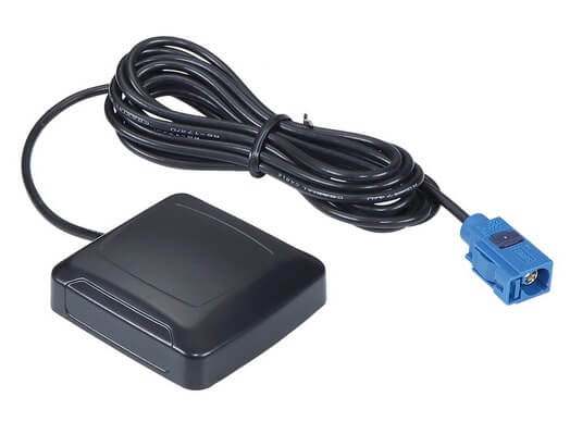
GPS antennas cURL Too many subrequests.
cURL Too many subrequests.
cURL Too many subrequests.
cURL Too many subrequests.
cURL Too many subrequests.
cURL Too many subrequests.
cURL Too many subrequests.
cURL Too many subrequests.
cURL Too many subrequests.