 Skip to content
In our increasingly connected world, the demand for reliable and efficient wireless communication continues to grow. Enter the PCB antenna, a sophisticated yet often overlooked hero in the vast arena of wireless technologies. This article delves into the essence of PCB antennas, exploring their functions, benefits, and applications across various industries.
A PCB (Printed Circuit Board) antenna is an essential component designed to transmit and receive electromagnetic signals within a device. Integrated directly into the PCB layout, these antennas utilize the board’s conductive traces to function, offering a compact and efficient solution for wireless communication.
Now that we understand what a PCB antenna is, let’s explore how exactly it functions within electronic devices and why its design is pivotal for the efficacy of modern wireless communication systems.
How Does the PCB Antenna Work?
PCB antennas are designed using conductive traces on a printed circuit board. These traces are typically made of copper and are arranged in specific patterns to form the antenna structure. The shape and size of the traces determine the antenna’s resonant frequency and radiation pattern.
When a signal is applied to the PCB antenna, it generates an electromagnetic field around the conductive traces. This field consists of electric and magnetic components, which propagate away from the antenna as electromagnetic waves.

The conductive traces act as a transmission line, carrying the electromagnetic waves along their length. As the waves propagate through the traces, they generate an electric field that oscillates at the antenna’s resonant frequency. This oscillating electric field then radiates into space, creating an electromagnetic wave that can be received by other antennas or devices.
Similarly, when an electromagnetic wave from another antenna or device reaches the PCB antenna, the conductive traces capture the wave’s electric field. This induces a current in the traces, which can be extracted and used as a received signal.
The size and shape of the conductive traces on the PCB antenna are crucial for its performance. They need to be carefully designed to match the desired frequency of operation. The length of the traces should be a fraction of the wavelength of the desired frequency, typically a quarter or half wavelength. This ensures that the antenna efficiently radiates or captures electromagnetic waves at the desired frequency.
Key Design Considerations for PCB Antennas
While the fundamental operation of a PCB antenna hinges on its conductive traces, several additional design factors play a pivotal role in its efficiency and effectiveness:
Positioning on the PCB
Where you place the antenna matters. Corners of the PCB are often ideal locations, as they allow for multiple transmission and reception directions, enhancing overall performance. However, the application and device layout can influence the final position.
Size and Weight Constraints
PCB antennas are prized for their compactness and light weight. When designing for portable or wearable devices, it’s essential to ensure the antenna does not exceed acceptable limits for size and weight, preserving the device’s overall form factor.
Ground Plane Design
The ground plane beneath or around the antenna must be sized appropriately. An insufficient or poorly placed ground can distort the antenna’s radiation pattern, undermining the efficiency of the entire RF circuit.
Component Clearance
To prevent interference, keep other electronic components, mounting screws, and metallic parts at a reasonable distance from the antenna. Close proximity to such elements can degrade signal transmission and reception.
Transmission Line Layout
The transmission line—essentially the path that carries the RF signal—should be as straight as possible. Bends or unnecessary length can introduce signal loss or degradation, impacting overall antenna performance.
In summary, PCB antennas work by using their conductive traces to generate or capture electromagnetic waves. The size and shape of the traces determine the antenna’s resonant frequency, enabling it to operate at specific frequencies for efficient communication.
In summary, PCB antennas work by using their conductive traces to generate or capture electromagnetic waves. The size and shape of the traces determine the antenna’s resonant frequency, enabling it to operate at specific frequencies for efficient communication.
Key Types of PCB Antennas and Their Distinct Features
PCB antennas come in a diverse array of designs, each with unique structural characteristics and specific advantages that make them suited to particular applications. Understanding these distinctions helps engineers and product designers select the optimal antenna type for their project. Let’s take a closer look at the most notable varieties:
Monopole Antennas
A monopole PCB antenna is constructed with a single straight conductor—often just a slender copper trace. Its straightforward design not only simplifies manufacturing and reduces costs, but also provides omnidirectional coverage, making it a practical choice for situations requiring a wide area of reception or transmission.
Monopole Antennas
Dipole antennas, in contrast, use two conductive elements of equal length arranged in a straight line. This configuration allows the dipole to radiate efficiently in two opposite directions, delivering a bidirectional pattern that’s ideal for certain wireless applications.
Patch Antennas
Patch antennas, frequently seen as flat metallic “patches” on the PCB, can take on rectangular, circular, or other geometric shapes. While they tend to be somewhat larger, these designs offer high gain and are particularly valued for their effectiveness in point-to-point links and applications demanding directional signal strength, such as GPS receivers.
Loop Antennas
When the conductive trace is fashioned into a closed-loop, the result is a loop antenna. These compact designs are easier to implement, though they generally exhibit lower efficiency. They’re ideal for situations where space is at a premium and simplicity is prioritized over maximum range.
Helical Antennas
Helical antennas stand out due to their coiled, spring-like conductive trace. This spiral structure allows the antenna to deliver higher gain and directional coverage, even in tight spaces, making these antennas valuable for portable devices and applications that benefit from a narrow transmission beam.
Slot Antennas
Slot antennas are formed by cutting a slot or gap into the conductive layer of the PCB. As electromagnetic energy interacts with the slot, it radiates efficiently. These antennas offer design flexibility and can be integrated into compact systems with minimal protrusion beyond the board.
Yagi Antennas
Yagi antennas incorporate a central driven element with additional parasitic elements (directors and reflectors) lined up on the PCB. This arrangement provides notably high gain and strong directional focus, at the expense of a larger physical footprint—a trade-off often worthwhile for long-range communications.
Planar Inverted F Antennas (PIFA)
Resembling a flattened and upturned letter “F” on the circuit board, the planar inverted F antenna (PIFA) is a go-to for modern, space-constrained devices like smartphones. It provides both high efficiency and an omnidirectional pattern, while keeping the required footprint to a minimum.
Meander Line Antennas
Meander line antennas solve space challenges by folding the trace back and forth in a zigzag path, significantly shortening the overall footprint. However, designers must carefully balance these space savings against potential impacts on the antenna’s radiation efficiency and pattern.
cURL Too many subrequests.
cURL Too many subrequests.
cURL Too many subrequests.
cURL Too many subrequests.
- cURL Too many subrequests. cURL Too many subrequests.
- cURL Too many subrequests. cURL Too many subrequests.
- cURL Too many subrequests. cURL Too many subrequests. L cURL Too many subrequests., c cURL Too many subrequests., f cURL Too many subrequests. cURL Too many subrequests. cURL Too many subrequests.
- cURL Too many subrequests. cURL Too many subrequests.
cURL Too many subrequests.
cURL Too many subrequests.
Creating Schematics and Layout for a PCB Antenna
Designing an effective PCB antenna begins with meticulous schematics and a thoughtfully optimized layout. Using industry-standard design software such as Altium Designer, KiCad, or Eagle, engineers start by drafting the schematic, carefully selecting and placing the necessary components while defining all the signal paths relevant to the antenna.
The next critical step is translating the schematic into a physical layout on the PCB itself. This involves arranging the antenna elements and associated circuitry in a manner that not only fits the device’s form factor but also supports optimal signal transmission and reception. Trace widths, spacing, and the position of ground planes must be precisely engineered to match the target operating frequency and ensure minimal loss and interference.
Engineers also utilize simulation tools to predict how the antenna will behave in the real world, allowing iterations on the design before moving to production. Attention to detail is crucial here—proper impedance matching and isolation from noisy components on the board can make a world of difference in real-world performance.
By carefully balancing the electrical and physical requirements, a well-crafted schematic and layout set the foundation for a high-performing PCB antenna, setting the stage for reliable wireless connectivity in everything from wearable devices to industrial applications.
Key Electrical Requirements for PCB Antenna Design
When designing a PCB antenna, it’s essential to ensure it meets specific electrical requirements tailored to its intended function and environment. Here are the primary considerations:
- Operating Frequency: The antenna must be precisely designed for the frequency range it will transmit and receive. This involves carefully calculating the trace lengths and shapes to match the desired frequency—typically expressed in megahertz (MHz) or gigahertz (GHz).
- cURL Too many subrequests. The appropriate radiation pattern depends on whether the application needs the antenna to radiate energy in all directions (omnidirectional) or focus energy in a particular direction (directional). The pattern must suit the device’s operational context to maximize signal reliability.
- Impedance Matching: For optimal performance, the antenna’s impedance should be matched to that of the transmitter or receiver—typically 50 ohms. Proper impedance matching minimizes signal reflection and maximizes power transfer.
- Polarization: Matching the polarization (the orientation of the electric field) between communicating devices enhances performance. Most PCB antennas use linear polarization, but some applications may require circular polarization.
- Bandwidth: The antenna should have sufficient bandwidth to support the intended communication protocol, whether narrowband or wideband operation is required.
Neglecting these electrical parameters can lead to suboptimal range, interference issues, or signal loss, emphasizing the importance of meticulous design at this foundational stage.
How Do You Choose the Type and Board Material for a PCB Antenna?
Selecting the right PCB antenna starts with understanding your device’s requirements and constraints. The antenna type—such as monopole, dipole, patch, or loop—should align with your intended function, preferred radiation pattern, and available space. For example, a monopole antenna may suit compact IoT gadgets, while dipole or patch designs can address broader bandwidth or directional needs.
Equally important is the choice of board material. Common options include FR4, Rogers, and other specialty substrates. Each material offers distinct electrical properties that impact antenna efficiency and signal integrity. While FR4 is cost-effective and widely used, higher-performance substrates like Rogers or Teflon provide lower dielectric losses, benefiting high-frequency or precision applications. Consider factors like frequency range, mechanical durability, manufacturing cost, and size when making your selection.
Thoughtful selection of both the antenna structure and board material lays the foundation for robust, efficient wireless performance in your device.
What Are the Main Steps Involved in Designing a PCB Antenna?
Designing a PCB antenna is a meticulous process, balancing technical precision with creative problem-solving. Let’s break down the essential steps involved to achieve optimal performance:
1. Select the Antenna Type and Board Material
Begin by identifying the best antenna structure for your application—choices may include monopole, dipole, patch, or loop designs. The specific type you choose will depend on required radiation patterns, frequency bands, operational bandwidth, and the space constraints of your device.
Next, choose an appropriate PCB substrate material, such as FR4 or Rogers laminates. The material selection directly influences the antenna’s electrical performance (like dielectric constant), mechanical durability, and overall cost.
2. Determine Antenna Dimensions
Precise sizing is crucial for PCB antennas. Calculate the height, width, and length of the antenna traces based on your target operating frequency and substrate properties. The resonance of the antenna is typically achieved with trace lengths at a quarter or half the wavelength of the intended frequency. Use standard formulas to fine-tune the width and length, taking into account the dielectric constant and thickness of your chosen PCB substrate.
3. Define Electrical Requirements
Establish the operating frequency, desired radiation pattern, polarization, and impedance. These parameters are fundamental in guiding the antenna’s design and ensuring compatibility with the rest of your wireless circuit.
4. Develop Schematics and Layout
Use professional PCB design software to create detailed schematics and lay out the antenna on your circuit board. This ensures the integration of all relevant components, optimal trace routing, and minimal interference or signal loss.
5. Perform Simulations and Validations
Before proceeding to physical prototypes, simulate the antenna using electromagnetic simulation software such as ANSYS HFSS, CST Studio Suite, or Keysight ADS. Simulations reveal potential issues in the design—allowing adjustments to be made early, which saves time and resources.
Each of these steps is integral to producing a high-performance PCB antenna, tailored to your specific application and optimized for reliable wireless communication.
The Importance of Design Simulation in PCB Antenna Development
Before moving from concept to production, simulating your PCB antenna design is a crucial step. Through simulation, engineers are able to identify and resolve potential issues long before a physical prototype is ever created. This minimizes costly mistakes, optimizes performance, and saves valuable development time.
Simulation software—such as ANSYS, CST Studio Suite, and HFSS—allows designers to model electromagnetic behavior, evaluate radiation patterns, and verify that the antenna will resonate at the intended frequency. By leveraging these powerful tools, you can visualize how your antenna will interact with its environment and ensure that it meets all performance requirements.
Ultimately, design simulation is an essential safeguard, ensuring that each PCB antenna not only meets functional expectations but is also tuned for the efficiency, reliability, and compactness that today’s wireless applications demand.
What is a PCB Antenna Used For?
PCB antennas are used for wireless communication purposes. They are designed to transmit and receive radio frequency signals, allowing devices to connect to networks or communicate with other devices wirelessly. Some common applications of PCB antennas include:
1. Wireless connectivity: PCB antennas are used in devices like smartphones, tablets, laptops, and smartwatches to provide Wi-Fi, Bluetooth, and other wireless connectivity options.
2. Internet of Things (IoT) cURL Too many subrequests.

cURL Too many subrequests.

cURL Too many subrequests.
cURL Too many subrequests.
cURL Too many subrequests.
cURL Too many subrequests.
cURL Too many subrequests.
cURL Too many subrequests.
cURL Too many subrequests.
- cURL Too many subrequests. cURL Too many subrequests.
- cURL Too many subrequests. cURL Too many subrequests.
- cURL Too many subrequests. cURL Too many subrequests.
- cURL Too many subrequests. cURL Too many subrequests.
cURL Too many subrequests.
cURL Too many subrequests.
2. Cost-effective: PCB antennas are relatively inexpensive to manufacture compared to other types of antennas, such as external or embedded antennas.
3. Easy integration: PCB antennas can be directly integrated into the PCB of the device, eliminating the need for additional external components or connectors. This makes the integration process simpler and more efficient.
4. Customizability: PCB antennas can be easily customized and optimized for specific frequency bands or performance requirements. They can be designed to have specific radiation patterns or gain characteristics, allowing for better signal reception or transmission.
5. Good performance: When properly designed and implemented, PCB antennas can provide good performance in terms of gain, efficiency, and radiation pattern. They can offer reliable wireless connectivity and communication.
6. Durability: PCB antennas are typically more robust and durable compared to external antennas, as they are protected within the device’s housing. They are less prone to damage or breakage.
7. Versatility: PCB antennas can be used in a wide range of applications, including wireless communication devices, IoT devices, mobile phones, tablets, laptops, and other electronic devices that require wireless connectivity.
8. Low power consumption: PCB antennas are designed to have low power consumption, which is essential for battery-powered devices. They can help extend the battery life of portable devices.
9. Compliance: PCB antennas can be designed to comply with regulatory requirements and standards for wireless communication, ensuring that the device meets the necessary certification and approval criteria.
10. Aesthetics: PCB antennas can be hidden within the device’s PCB, resulting in a cleaner and more aesthetically pleasing design.
Considerations and Drawbacks
While PCB antennas offer many advantages, it’s important to note a few limitations:
- Efficiency and bandwidth: The compact size that makes PCB antennas so appealing can also limit their bandwidth and reduce overall efficiency compared to larger or external antennas.
- Environmental interference: Being integrated within the device, PCB antennas can be more susceptible to interference from other electronic components or from external factors such as proximity to metal objects.
- Design complexity: Achieving optimal performance often requires careful design and tuning to match the desired frequency bands while minimizing losses.
Despite these potential drawbacks, the benefits of PCB antennas—cost, integration, and compactness—often outweigh the challenges, especially for devices where space and efficiency are at a premium.
What Are the Disadvantages of a PCB Antenna?
While PCB antennas offer many benefits, they also come with a few trade-offs that are important to consider:
- Limited bandwidth: Due to their small and compact design, PCB antennas often have a narrower bandwidth compared to larger or external antennas. This can restrict the range of frequencies over which they perform optimally.
- Potentially lower efficiency: Miniaturization can sometimes lead to less efficient signal transmission or reception, especially when space constraints limit the physical size of the antenna elements.
- Sensitivity to environment: PCB antennas may be more susceptible to detuning or performance shifts caused by nearby components, the device enclosure, or changes in the surrounding environment. This can lead to variability in wireless performance.
- Design complexity: Achieving optimal performance often requires precise design, careful layout, and proper grounding on the PCB. Small design changes can have a significant impact on antenna characteristics.
- Reduced range: In some cases, the effective communication range of a PCB antenna may be shorter than that of larger, external antenna types.
Despite these limitations, with careful engineering and consideration of application needs, PCB antennas remain a popular choice in many modern electronic devices.
What is the Frequency of a PCB Antenna?
The frequency of a PCB (Printed Circuit Board) antenna refers to the resonant frequency at which the antenna is designed to operate optimally. It is the frequency at which the antenna radiates or receives electromagnetic waves most efficiently. The frequency of a PCB antenna can vary depending on the specific design and application, but it is typically in the range of a few megahertz (MHz) to several gigahertz (GHz).
Typically, PCB antennas operate at high frequencies, such as the 2.4 GHz ISM band, commonly used in WiFi and Bluetooth applications. The design can be tuned to various frequencies depending on the specific needs of the device.
What is the Gain of a PCB Antenna?
The gain of a PCB antenna is typically measured in dBi (decibels relative to an isotropic radiator). An isotropic source radiates power equally in all directions, so a higher gain indicates that more of the antenna’s power is directed in a specific direction.
PCB antennas typically have gain values ranging from 0 dBi to 6 dBi. A gain of 0 dBi means that the antenna radiates power equally in all directions, like an isotropic source. A gain of 6 dBi means that the antenna radiates power in a more focused direction, resulting in a stronger signal in that direction.
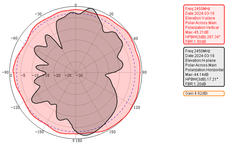
The gain of a PCB antenna is influenced by its physical design, such as the size and shape of the antenna elements, as well as the materials used in its construction. The gain can also be affected by the environment in which the antenna is placed, such as nearby objects or the presence of obstructions.
It’s important to note that while gain is a measure of the antenna’s efficiency in directing power, it does not indicate the total power radiated by the antenna. The total radiated power depends on the input power to the antenna and the antenna’s efficiency.
What is the Difference Between a Wire Antenna and a PCB Antenna?
A wire antenna is a type of antenna that consists of a conductive wire that is used to transmit and receive radio frequency signals. It is typically made of copper or aluminum and is designed to be resonant at a specific frequency or a range of frequencies. Wire antennas are usually installed outdoors and can be in the form of a dipole, monopole, or loop.
On the other hand, a PCB (Printed Circuit Board) antenna is a type of antenna that is integrated into a printed circuit board. It is typically made of conductive traces that are printed onto the PCB using a special process. PCB antennas are compact in size and can be designed to be highly directional or omnidirectional. They are commonly used in small electronic devices such as smartphones, tablets, and wireless routers.
cURL Too many subrequests.
cURL Too many subrequests.
A cURL Too many subrequests. cURL Too many subrequests.
cURL Too many subrequests.
cURL Too many subrequests.
cURL Too many subrequests.
cURL Too many subrequests.
cURL Too many subrequests.
cURL Too many subrequests.
cURL Too many subrequests.
- cURL Too many subrequests.
- cURL Too many subrequests.
cURL Too many subrequests.
cURL Too many subrequests.
cURL Too many subrequests.
cURL Too many subrequests.
cURL Too many subrequests.
cURL Too many subrequests.
– PCB antennas can be more complex to design and integrate into the PCB layout compared to chip antennas.
– They require careful consideration of the PCB material, size, shape, and ground plane for optimal performance.
- While PCB antennas tend to cost less than chip antennas and can produce stronger signals with higher bandwidth, they generally take up more space on the board and can be more susceptible to environmental interference.
In summary, the main difference between a chip antenna and a PCB antenna is their physical form and integration into the PCB. Chip antennas are small, compact components that are surface-mounted onto the PCB, offering ease of integration and resistance to some environmental effects, while PCB antennas are printed or etched directly onto the PCB itself, typically providing higher gain and bandwidth but requiring more design considerations and space.
Overall, PCB antennas are becoming more important as technology advances. They provide a flexible and effective option for wireless communication in small devices. Whether for personal or industrial use, knowing the benefits and capabilities of PCB antennas can greatly improve device design and performance.